Chiplets are small, modular integrated circuits that can be combined to form a large system-on-chip. Differing from the conventional monolithic integrated circuits, which are fabricated by using a single piece of large silicon connect, the chiplets are fabricated separately and interconnected using advanced packaging techniques. The modular approach brings in flexibility in design and manufacturing.
Distinguishing features from the traditional monolithic chips:
Modularity: Solutions can be made from individual chiplets mixed and matched to be tailor-made, but monolithic chips are monolithic — indivisible.
Manufacturing Efficiency: Chiplets are able to use process nodes optimized independently for performance and cost, while monolithic chips are forced to use a single process node for the entire chip.
Scalability: It is easier to scale performance by adding or upgrading individual components without redesigning the whole chip using chiplets.
Yield Improvements: Manufacturing yields for small chiplets are better than for a few large monolithic chips; hence it leads to cost reduction and waste minimization.
Historical Background

The advancement in chip design has primarily been led by a pursuit of enhanced performance, efficiency, and cost-effectiveness. To this end, a quick overview of historical advancements in chip design before the recent rise of chiplets is articulately detailed as below:
Early Integrated Circuits: 1960s-1970s — the first developed integrated circuits were pretty much simplistic, having relatively few transistors on board. With technology improvement and upgrades, so did the number of available transistors on one chip, which developed into complex monolithic chips.
Moore’s Law (1970s-2000s): Made in 1977, Gordon Moore’s observation that the number of transistors on a chip would double about every two years was proved right and held true for a few decades, meaning exponential growth in performance and complexity of chips.
Challenges of Scaling (2010s): Transistor sizes approached nearly atomic dimensions, due to which scaling down the feature size became increasingly difficult and expensive. Power dissipation, power consumption, and process defects — difficulties like heat dissipation — were getting quite pronounced at that point.
Chiplets, 2010s to present: Faced with the challenge, the industry began to explore alternatives. It became popular that what would work was chiplets, a method to increase performance and efficiency without the monolithic scaling limitations. Advanced packaging techniques were developed for interconnecting chiplets effectively by companies such as AMD and Intel at the forefront.
Architecture
Chiplet architecture refers to the design philosophy for smaller, independent modular IC chiplets that can be put together to build a bigger, more complex system.
The following is a full description of their composition and interconnection details:
Modular Design: In this basic concept, every chiplet was meant to feature a given task: processing, memory, or I/O. The chiplets could be independently developed and tailored for the specific needs of their functions.
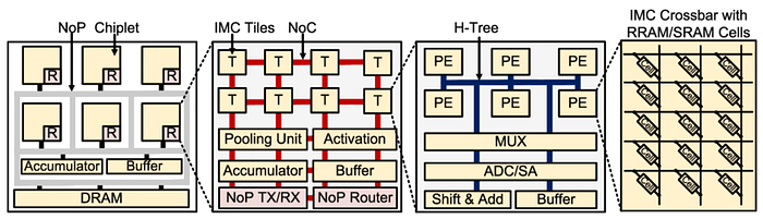
Interconnects: At the heart of the chiplet model lies the interconnect technology that ties the individual chiplets together. Here, the use of silicon interposers and through-silicon vias is done to marshal high bandwidth with low latency among chiplets. All in all, interconnects enable the chiplets to communicate well and transfer data efficiently.
Heterogeneous Integration: Such a technique makes it possible to fabricate chiplets using different process nodes and different materials to allow for heterogeneous integration. What this means is that high-performance logic chiplets could be combined with memory chiplets or analog components.
Scalability and Flexibility: The designs can be scalable and flexible due to the modularity of the chiplet; an increased number of additional functionalities can be realized by including additional chiplets and advances in chiplets can be upgraded without redesigning the whole system.
Manufacturing of Interposer-based Chiplets
Manufacturing of chiplets is quite different from the traditional monolithic chip manufacturing process:
The technology enables different chiplets to be manufactured separately, most likely using different process nodes that are optimized for their independent functions. This way, the respective best technology for each device can still be applied with more freedom.
The advanced packaging techniques that were designed to enable the assembly of chips at the wafer level are applied to chiplets that have emerged from their respective fabrication process, where the chiplets are placed on a silicon interposer or directly on a substrate. That is, on such a substrate, the chiplets are interconnected across the silicon with TSVs or any other form of high-density interconnect.
Since chiplets are small in size and less complicated than the monolithic chip, they typically have a better manufacturing yield. Testing of each chiplet can be performed before their integration to ensure that, in the end, only chiplets with active functions are used, which reduces waste and increases the overall yield.
It includes the packaging of combined chiplets. It is the method of 2.5D or 3D stacking whereby chiplets are placed one over another or by the side on an interposer. The being a package is encapsulated and connected to the external circuitry.
Used Materials
Chiplet materials are selected based on their functionality and specific requirements from the interconnect technology. Among these, silicon continues to be the dominant substance for most of the chiplets, which are dedicated to logic, memory, and all semiconductor components. Silicon interposers are also involved in high-density interconnects.
Copper: Copper is applied in almost all interconnects because of its superior electrical conductivity. It is applied in TSVs and all other interconnect structures ensuring efficient data transfer between the chiplets.
Low-K Dielectrics: They are the materials used to isolate the interconnects and thereby reduce capacitance; this is done to increase the speed of signals and power consumption.
Advanced Packaging Materials: Organic substrates, epoxy resins, and underfill compounds provide the relevant mechanical support, thermal management, and protection for the chiplets during the process of packaging.
Specialized Materials: Some other materials, such as gallium arsenide or silicon carbide, are employed for some chiplets based on the application. This is in high-frequency or high-power applications.
Advantages of Chiplets
Scalability
The modular approach allows easy scaling up or down, where chiplets enable designers to come up with systems. In other words, much more functionality can be added with the integration of more chiplets without necessarily going through the redesigning of the whole system.
The different chiplets may be combined one with the others to tailor the solution to any specific application. Eg a supercomputing system may consist of many processor chiplets and memor and I/O chiplets other than a number of processor chiplets dedicated to that system and would, therefore, be optimally configured for the purpose.
That any new technology or an improvement in chiplet design be incorporated in a system without the system been entirely re-designed. This fact means the updating and improvement in life expectancy of electronic appliances.
Chiplets can be designed to work in parallel, distributing work across a number of them, thereby increasing the system processing power and optimization for aggressive applications, especially in areas of AI and machine learning.
By design, the architecture is parallel in nature, so that small units can operate collectively on a big integrated platform. This results in great cost efficiency, for example:
The yields for smaller chiplets are better than those of a big monolithic chip. This is because it is less likely that a defect will appear on the small chiplet, which considerably decreases scrap and thus reduces
By the use of chiplets, company can combine different components to deliver tailored solutions. This allows flexibility in choosing the most cost-effective process nodes for each component to achieve optimum performance at the lowest cost.
Reduced Development Costs Developing a new monolithic chip is expensive and time-consuming. With chiplets, a manufacturer can reuse existing designs and integrate them into new systems, which lowers development time and by extension the cost of development.
It costs an average of pennies per chip to make chiplets. The more chiplets to be churned at a given time will make more savings, and the cost per chiplet becomes very little.
Chiplets offer several performance benefits, including improved power efficiency and thermal management:
Optimized Performance: Each chiplet can be optimized for its specific function, whether it’s processing, memory, or I/O. This specialization allows for better performance compared to a monolithic chip that has to balance multiple functions.
Chiplets can be made to run on low power, which ultimately brings down the overall power consumed. Now, this is very pertinent to battery-driven gadgets, such as smartphones or laptops.
Thermal Management: Although smaller chiplets produce less heat compared to large monolithic chips, advanced packaging techniques like 3D stacking and the use of thermal interface materials further help in heat dissipation and hence improve the thermal performance of the system.
High Bandwidth Interconnects: Newer technologies related to interconnect, such as silicon interposers and TSVs, enable communication among chiplets at very high bandwidth. This ensures the easy and fast flow of data and, through this, lessens latency, which further enhances system performance in general.
Challenges and Limitations
Interconnect Complexity
One of the biggest challenges towards the development and application of chiplet technology is the complex process of interconnecting the individual chiplets. Some of these details include:
High-density interconnects: The high throughput needed for many chiplets also demands high-density interconnects for the conduction of high-speed data. Here come technologies through silicon vias and silicon interposers, but with their problems of inherent increased complexity and raised process costs.
Signal Integrity: Ensuring signal integrity across the interconnects is very important. Crosstalk, signal attenuation, and electromagnetic interference are some of the problems appearing at high data rates. Advanced design and testing techniques ensure reliable communication among the chiplets.
Power Delivery: The other point of challenge is in delivering power to each chiplet efficiently. Interconnects have to be designed in such a way that there is minimal loss in power with a stable power supply. This can be challenging because the connections are much denser and in smaller sizes.
Thermal Management: Therefore, the interconnects shall also dissipate heat effectively. Bad dissipation of heat through the interconnect may introduce hot spots and, with that, reduce the performance or reliability. Sometimes even advanced cooling solutions and thermal interface materials are necessary to solve the problem.
Design Complexity
System Integration: It has got to be considered that cramming multiple chiplets into a singlecohesive system is very much a matter of up-front planning and design. Each chiplet has to be optimized for its function and at the same time compatible with the other many chiplets in the system.
Design Tools and Methodology: The traditional design tools and methodology are hellishly insufficient to design chiplet based systems. The added-on complexity requires additional new tools and ways to make the design and verification process go on more efficiently.
Test and validation of chiplet-based systems are much more complex than in the case of monolithic chips. Each chiplet should be tested independently, and the total system should be validated toward function and performance. This requires advanced testing techniques and equipment.
Supply Chain Management: Coordination with multiple suppliers to fit compatible chiplets adds more complexity in terms of manufacturing coordination and logistics.
Standardization Challenge
There are strong standardization concerns with the chiplet industry.
Interoperability, without any standardized interfaces and protocols, is tough across chiplets from different manufacturers. This decreases the flexibility of the technology and to mix and match the chiplets.
It is a matter of joint interest to create an ecosystem around chiplets that are robust, involving the chip designers, manufacturers, and tool providers. With the absence of standardization, this kind of collaboration gets restricted, which, in turn, limits the adoption of the technology.
The development of custom interconnects and interfaces with different chiplets increase the cost and time to market of product design and product manufacturing. Standardization can help minimize these costs and cut the development process.
Different countries have different rule and standards for electronic parts. The absence of universal standards for chiplets can show further increase in the cost to meet particular regional standard and can restrict market of product to different countries.
Addressing these challenges and limitations is important for the success of chiplet technology and furthering its large-scale adoption. Overcoming these challenges will heavily rely on industry cooperation and the standardization of interfaces and protocols.
Applications
Data Centers
The role of chiplets in improving the performance and efficiency in data centers is of great importance.
Scalability and flexibility: Data centers house applications or workloads. A good attribute of chiplets is that they offer the flexibility to design a modular way, such that processing, memory, and input/output capabilities can be scaled separately. This won’t ensure flexibility in the design of what different-size tasks the data centres should accommodate — ranging from simple data storage to complex computational needs.
In this sense, high performance data centers can be made possible with embedded, specialized chiplets. In the placement of high-speed processing chiplets integrated with large-memory chiplets, the performance of data intensive applications takes a very serious step up.
Power Efficiency: One of the biggest worries about data centres is the amount of power they consume. Chiplets can be designed to operate at lower power input and hence lower the power consumption of the whole device. This worry is paramount for very large data centres in balancing costs on power and thermal outputs.
Enhanced Yields and Cost Efficient: The chiplets designed using modular architecture improve the yields and achieve cost efficiency in manufacturing. Data centers enjoy cost reduction and increased reliability by quick replacement of any malfunctioning chiplet without the need to dispose of the whole system.
Advanced Interconnects: High bandwidth interconnects between chiplets allow faster data transfer and low latency, which meets real-time data processing and high-performance computing requirements in the data center.
Consumer Goods
It is more the case that chiplets are likely to find increased use within the consumer electronics segment, mainly mobile phones and laptops, to enhance them both technically and functionally:
Consumer electronics require the newest compact design with high efficiency. The use of chiplets will make it possible to put a load of multiple functional integration into smaller form factors, making the devices, say smartphones and laptops, highly powerful and highly featured.
Customization and Differentiation: Manufacturers can mix and match different varieties of chiplets as a solution for customization in order to differentiate their products. For instance, in a smartphone, integration of a high-performance processing chiplet with a special-purpose AI chiplet can be realized for camera enhancements and user experiences.
Thermal Management : Because consumer electronics should retain performance and reliability, efficient thermal management is an important goal. On the other hand, chiplets produce less heat than monolithic chips can; advanced packaging techniques dissipate the heat better.
Future-Proofing : The modular way of making chiplets can allow the easy upgrading of devices and, in every sense, future-proofs consumer electronics. This means adding new functionalities can be added to devices by increasing the number of chiplets in them, meaning that the devices’ shelf life is increased.
AI and Machine Learning
For AI and machine learning, there are several benefits of using chiplets, which include the following:
Specialized Processing: It is a fact that AI and machine learning applications require specialized processing. Thus, chiplets may be created to aid inference or training neural networks, in turn allowing the most effective kind of processing to be achieved on the job.
Parallel Processing: Many AI applications require parallel processing of huge datasets. By design, chiplets can work parallel to each other by distributing the work between other units. This results in higher speed in processing tasks with improved efficiency.
High Bandwidth and Low Latency: AI and ML run in speeds associated with high bandwidth and very low latencies in data transfer. Advanced interconnects between chiplets ensure the efficient movement of data from one chiplet to another. This greatly improves the performance of AI systems.
Scalability: AI workloads are not uniform and could cover small-inference scales to the large-scale training of deep neural networks. For flexibility in providing the scalability needed for these variable AI workloads, chiplets provide flexible, efficient solutions.
An extended further enhancement to AI capabilities would be the integration with other technologies when the chiplets are integrated with such emerging technologies as quantum computing and neuromorphic engineering, which opens up new possibilities in advanced AI applications.
These are some ways in which the advantages of chiplets increase the performance, efficiency, and flexibility with which they work, thereby supporting wide innovation in the data centers and consumer electronics and various AI applications to boost their use across boards.
Future Trends
Advancements in Packaging
Future advances in packaging technologies will go a long way to benefit chiplets with further enhanced performance, efficiency, and integration capabilities:
Perhaps the most promising of these developments is 3D stacking, where chiplets are being stacked one on top of the other. The basic idea here is reducing the separation between chiplets for faster data transfer and lower latency. In addition, it allows for even more compact designs, which is very significant for space-constrained applications such as smartphones and wearables.
Advanced interposers: Though much work has been done in using silicon interposers for the purpose of chiplet connectivity, the future could enable an enhancement beyond current implementations by achieving aggressive density in interconnects and improved thermal management. This enables even more efficient communication between the different chiplets and supports higher performance.
Heterogeneous Integration: Future packaging technologies will continue to expand their ability to integrate chiplets built using different materials and process nodes. Such integration will be able to marry high-performance logic chiplets with other specialized chiplets in memory, analog, and RF to fully optimize the performance at the system level.
Embedded Multi-Die Interconnect Bridge (EMIB): It’s a high-density interconnect technology between chiplets without the need for a full silicon interposer. From this overview, future innovations using EMIB might be more flexible and might accrue larger performance benefits in chiplet-based systems.
Advanced Thermal Management: With increasingly more chiplets integrated into one die, thermal management becomes very important. The coming packaging solutions will have advanced thermal management solutions such as microfluidic cooling and advanced thermal interface materials to ensure reliable operation.
Integration with Other Technologies
Chiplets are poised to integrate with several emerging technologies, opening new possibilities and applications:
Quantum Computing: The operation of quantum computers actually requires highly specialized components and an environment with very low temperatures. The implementation of a quantum processor, designed with the use of chiplets, connects classic control and readout electronics with the quantum processors to produce hybrid quantum and classic computing.
Neuromorphic engineering is the science that tries its best in constructing hardware that mimics the neural structure inside a human’s head. To realize scalable, flexible neuromorphic designs, the approach introduced in this paper is to develop a modular neuromorphic system with chiplets to represent each hardware component corresponding to a neural network layer or function.
Photonics: Since the photonic chiplet uses light in place of electrical signals to transfer information, it can certainly be integrated alongside electronic chiplets. These integrated systems are most likely going to show ultra-high transfer rates and probably very low power-hungry systems, especially good for data centers and high-performance servers.
5G and Beyond: With 5G networks being deployed and future communication technologies being developed, the use of Chiplet Integration is limitless. Highly specialized RF and signal processing modules are created using Chiplets to enhance the performance and efficiency of this communication system.
AI and Machine Learning: Chiplets will play a critical role in delivering the quantum performance gains and efficiency required by the vogue in AI and machine learning applications. Specialised AI chiplets can be integrated with general-purpose processors to create powerful and efficient AI systems.
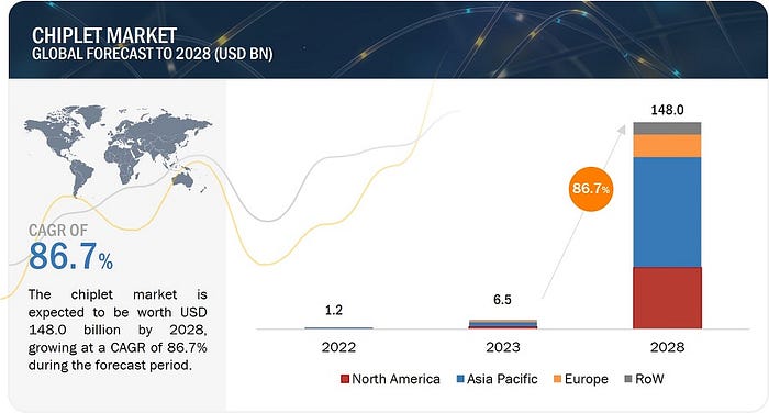
Market Growth
The market for chiplets is going to be significantly large because it will pool in growth coming from several areas:
Increasing Demand in High-Performance Computing: High-performance computing is in high demand, whether in data centers, AI, or machine learning, and it is what has chiplet technology at great proportions. Chiplets offer the scalability and performance that is driven by demand.
Cost Efficiency: The identified cost benefits of chiplets, allowing for better yields and the ability to merge and integrate elements, will generate high interest among many manufacturers. In a consumer electronics value chain, which is price-driven, this cost efficiency would be specifically crucial
Technological Advancements: The progress in packaging and interconnect technologies is constant, and it so remains even as of today. Tangible improvements are already transforming chiplets into an applicable and convincing reality. It is only after the maturity of these technologies that the implementation of chiplets is expected to be witnessed at an accelerated pace.
Investments: AMD, Intel, TSMC, and several others have major investment in developing this chiplet technology. These leading companies help provide an area for innovation and will most likely influence other companies to join the chiplet bandwagon.
Standards: All chiplet interfaces and protocols standardization will enable interoperability of components and hence lead to very much lower development costs. Standards developed and adopted will make it relatively easy for manufacturers to place many chiplets from several suppliers on the same plan.
Several companies have taken a lead in chiplet technology innovation and are well known for driving industry standards. Amongst them are:
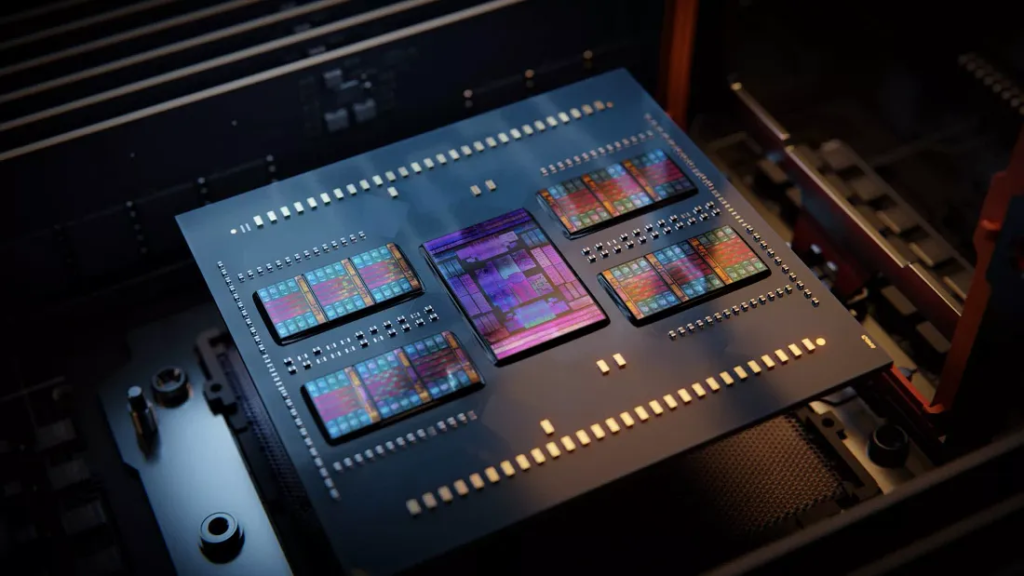
AMD: AMD has been very early with chiplet technology, starting from its first applications in Ryzen and EPYC processors. The company employs an MCM approach in designing the processors, where different chiplets are interconnected using an Infinity Fabric, which can involve high-performance CPU cores with other specialized chiplets, attaining the pinnacle of performance and efficiency.
Intel: Intel is another player who has been pioneering in the chiplet space. This company developed some of the advanced package technologies, such as EMIB (Embedded Multi-Die Interconnect Bridge) and Foveros. Through such high-density interconnects and chiplet 3D stacking, Intel can create powerful and efficient processors for a wide spectrum of applications.
TSMC: Taiwan Semiconductor Manufacturing Company (TSMC) is one of the leading semiconductor foundries that provide advanced packaging solutions for chiplets. TSMC applies its powerful CoWoS (Chip-on-Wafer-on-Substrate) and InFO (Integrated Fan-Out) packaging technologies to achieve the highest performance and greatest integration of the chiplets in the industry.
Current Use-Cases
This leading-edge chiplet technology has been electrically tested and validated in the following industries so far:
Datacenters: AMD’s EPYC processors for datacenters make an exemplary case of chiplet structure: Its processors have many CPU chiplets bunched together with one central I/O die — towards high performance, scalability, and power efficiency. This kind of architecture has, in fact, received good acceptance in the data center market, owing to substantial improvements over the implementations of monolithic design.
Consumer Electronics: Examples of where chiplet technology is found in the consumer electronics space are with Apple products such as the M1 and M1 Pro/Max. These chips are based on SoCs that combine various chiplets — like the CPU, GPU, and neural engine — into one package. So far, this has been Apple’s strong selling point, with both performance and power efficiency high, making it a strong competitor in the market for consumer use.
AI and Machine Learning: The technology of chiplets operates victoriously in another area for NVIDIA: its A100 Tensor Core GPU. The A100’s part of a multi-chip module, marrying GPU chiplets to process massively AI and machine-learning workloads. The architecture opens up ways for NVIDIA to build high-performance and energy-efficient data centers and solutions in research organizations.
Future Outlook
The future of chiplet technology is definitely exciting with ongoing developments in packaging, interconnects, and integration with upcoming technologies. As the industry is scaling towards applications that are more complex and demanding, in the future, the chiplets will play a pivotal role in dealing with these challenges. With standardization of interfaces and protocols, growth is going to be immense and the use of chiplets will be ubiquitous, to make it a cornerstone of the next generation of semiconductor design.